

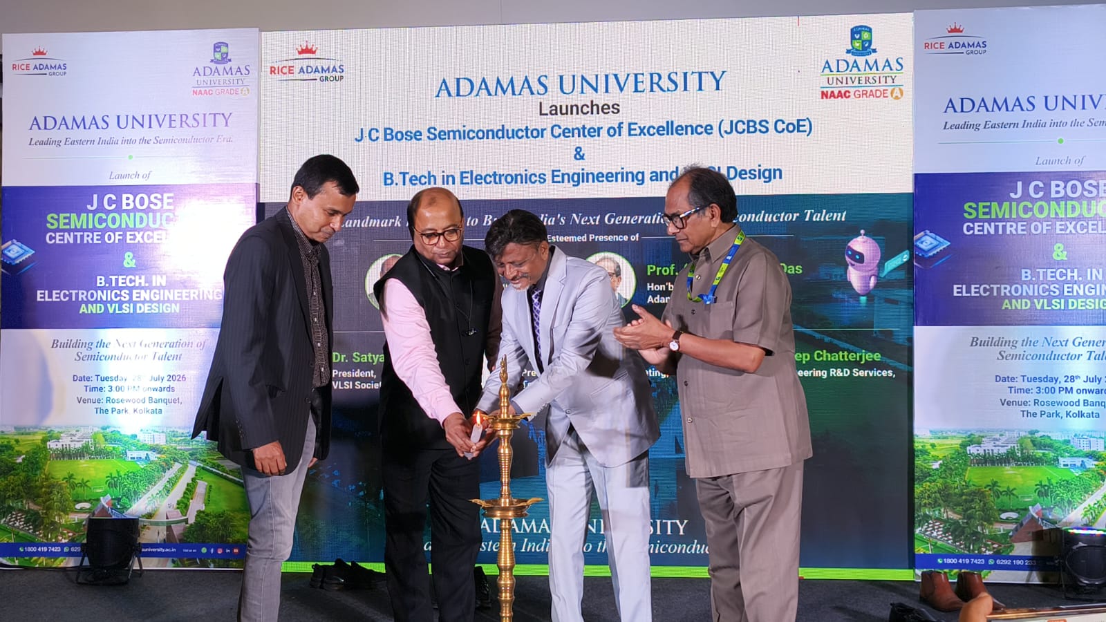
Kolkata, July 28: Seeking to bridge India’s growing semiconductor talent gap, Adamas University on Tuesday announced an investment of ₹10 crore over the next five years to establish Eastern India’s first J. C. Bose Semiconductor Center of Excellence (JCBS CoE) and launched a new B.Tech. in Electronics Engineering with VLSI Design, an industry-aligned undergraduate programme designed to develop the next generation of chip designers and semiconductor engineers.
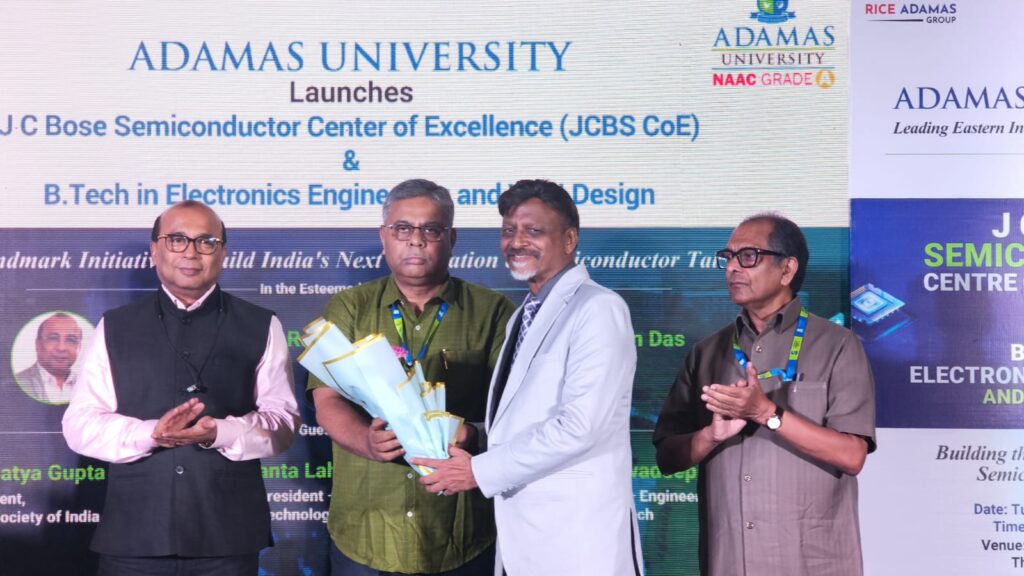
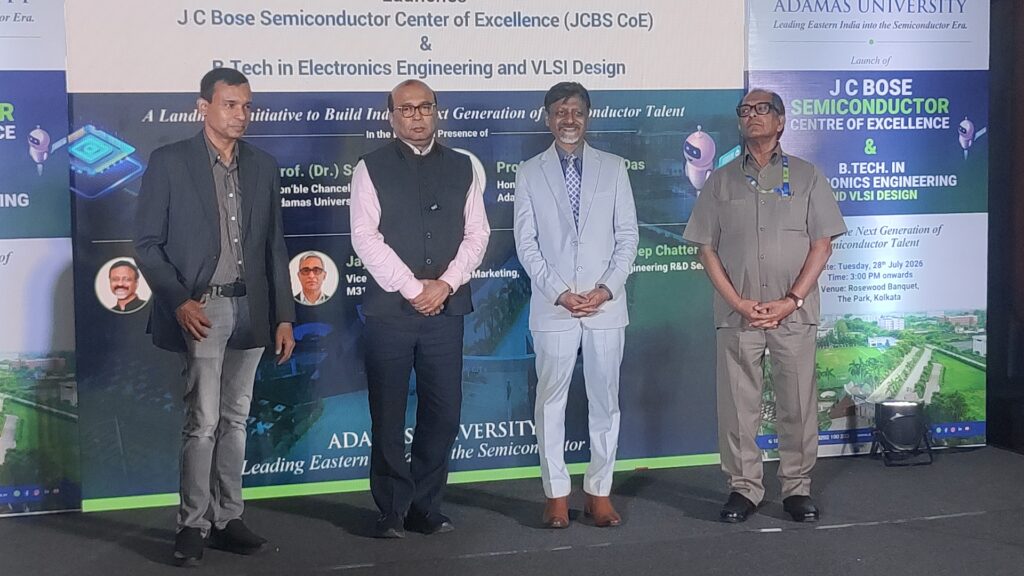
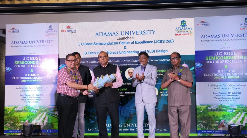
The initiative was unveiled at a city hotel, Kolkata, in the presence of Prof. (Dr.) Samit Ray, Chancellor, Adamas University; Prof. Suranjan Das, Vice Chancellor; Dr. Satya Gupta, President, VLSI Society of India; Biswadeep Chatterjee, AVP – Engineering R&D Services, HCLTech; and Jayanta Lahiri, Vice President – Technical Marketing, M31 Technology.
The university said the J. C. Bose Semiconductor Center of Excellence (JCBS CoE) will function as an integrated hub for advanced semiconductor education, research, innovation and industry collaboration, providing students with access to specialised laboratories, industry-standard EDA tools, FPGA prototyping facilities, internships, live projects and mentorship from leading semiconductor professionals.
The four-year, 162-credit B.Tech. in Electronics Engineering with VLSI Design has been developed in close consultation with industry and covers the complete semiconductor value chain, including VLSI design, AI hardware accelerators, FPGA systems, SystemVerilog/UVM verification, physical design, IC fabrication, static timing analysis, semiconductor packaging and embedded systems. The curriculum also incorporates laboratory-based learning, industry projects and a capstone project to equip graduates with practical skills.
The launch comes as India accelerates investments in semiconductor manufacturing and chip design under the India Semiconductor Mission (ISM) 2.0, creating strong demand for skilled professionals across chip design, verification, fabrication, testing and packaging.
Prof. (Dr.) Samit Ray, Chancellor, Adamas University, said the university’s vision extends beyond producing employable graduates.
“Our objective is to build an ecosystem where education, research, innovation and industry work together to create globally competent semiconductor professionals. We aspire to nurture future researchers, entrepreneurs and technology leaders who will contribute to India’s emergence as a global semiconductor hub.”
Prof. Suranjan Das, Vice Chancellor, Adamas University, said the J. C. Bose Semiconductor Center of Excellence (JCBS CoE) would serve as a strategic platform for industry-driven research and innovation.
“The curriculum has been developed with strong industry participation and significant practical exposure so that graduates are equipped to meet the rapidly evolving needs of the global semiconductor industry.”
Dr. Satya Gupta, President, VLSI Society of India, said Bengal occupies a unique place in the history of semiconductor science.
“It was in Kolkata in 1898 that Acharya J. C. Bose developed the world’s first solid-state semiconductor diode. To honour this pioneering legacy, we are proud to launch the B.Tech. in Electronics Engineering with VLSI Design and the J. C. Bose Semiconductor Center of Excellence (JCBS CoE) at Adamas University. Under the leadership of Dr. Samit Ray, Adamas University will invest INR 10 crore in this initiative over the next five years, aligning with the India Semiconductor Mission to help build a self-reliant semiconductor ecosystem.”
He added that the initiative is supported by MeitY’s Chips to Startup (C2S) programme and the ChipIN Centre, enabling students to access industry-standard EDA software, FPGA prototyping laboratories and advanced semiconductor testing equipment.
“Over the next five years, the programme aims to train 1,000 industry-ready students, upskill 100 professionals and achieve 10 full System-on-Chip (SoC) student tape-outs on advanced technology nodes. A student-led semiconductor club will promote hands-on innovation, while the J. C. Bose Semiconductor Center of Excellence (JCBS CoE) will serve as an incubation hub for fabless start-ups and indigenous semiconductor products and intellectual property creation. By connecting Bengal’s scientific legacy with modern VLSI education, we are empowering local talent to strengthen India’s semiconductor capabilities and contribute to the vision of Viksit Bharat 2047. Yahi Samay Hai – Sahi Samay Hai.”
Biswadeep Chatterjee, AVP – Engineering R&D Services, HCLTech, said the programme would provide students with exposure to the complete semiconductor design lifecycle through industry-mentored projects.
“This is among the few undergraduate programmes built around end-to-end VLSI. Students will gain hands-on experience with industry-standard design flows and tools while working alongside practising engineers.”
Jayanta Lahiri, Vice President – Technical Marketing, M31 Technology, described the J. C. Bose Semiconductor Center of Excellence (JCBS CoE) as a landmark initiative that will significantly strengthen semiconductor education, research and industry collaboration in Eastern India.
With the launch of the J. C. Bose Semiconductor Center of Excellence (JCBS CoE) and the B.Tech. in Electronics Engineering with VLSI Design, Adamas University aims to become a major contributor to India’s semiconductor ecosystem by developing industry-ready talent, promoting applied research and fostering innovation in advanced electronics.